


High Frequency Electronics (HFE) Lab, was founded in 2001 by inheriting ten years of experience in the area of modeling and design of microwave electronic circuits. This experience has been further exploited and finalized to several technological and scientifc challenges. Among them it is worth mentioning those running at present:
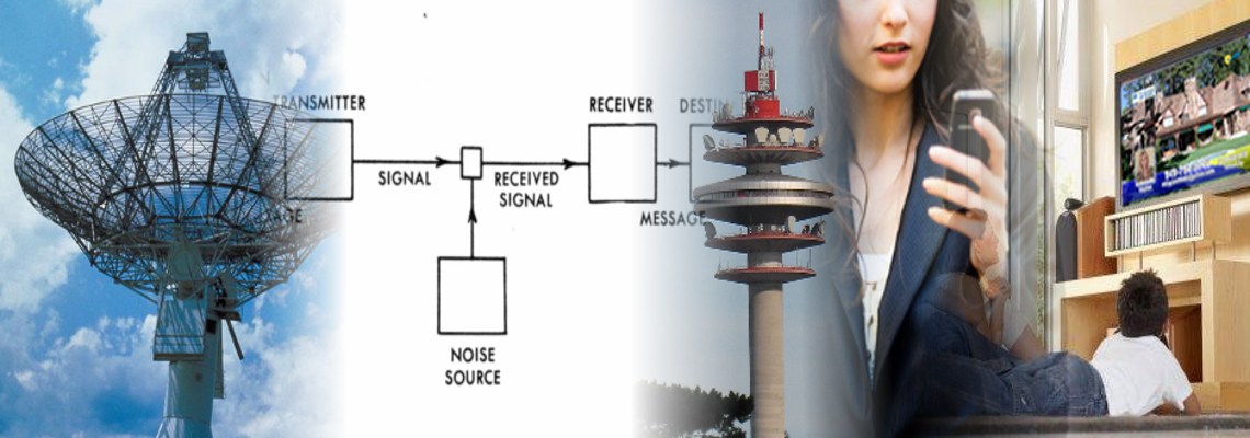
RFID systems
RFID concept has been introduced during WWII to identify flying objects (IFF systems), now they in many daylife areas (logistics, monitoring, counterfighting, survelliance, access regulation, and so on). This wide diffusion is posing continuous challenges, stimulates new applications and suggests new solutions to old problems. The HFE activity in this area is mostly devoted to develope innovative architectures (harmonic RFID, chipless Tags, ...) new materials (paper substrates, organic semiconductors, bioplastics, ...) to anable new RFID solutions related to the emerging Internet of Things (IoT) and Wide Area Electronics (WAE) scenarios.
Systems in Package (SiP) on Paper (SiPoP)
SiP is an approach first developed by using Low Temperature Cofired Ceramic (LTCC) material. that allow multilayer microwave elctronic circuits with controlled buried metallizations to be realized. Ultimately even the package can be realized with a selective grow of controlled layers thus resulting in a structure where package and circuit can be seen as a whole, suggesting the name SiP. This approach can be easily extended to the use of paper as the reference substrate; in this case we can thus speak about SiP on Paper (SiPoP)
Green Electronics
Green electronics is a filosophy more than a technology. It represents a new mentality to look at the development of electronics. The need of this revolution is a consequence of the appearence of new ideas often summarized under the definition of Internet of Thing. Actually, if we are going to increase the volume of electronics in the world, according to IoT evolution, without the possibility to localize precisely neither collect them at the end of life cycle, we have to develope these systems in a ecofriendly way. Ecofrindly means actually two things: biodegradable and zero energy impact. These two aspects imply: the use of biodegradable materials and the energy athonomy respectively. Techonologically speking this leads to some keywords: energy scavenging, low power circuits, organic semiconductors, paper circuits, and so on. The most of the activity in this field is devoted to develop electronic solutions for societal needs according to these ecofriendness constraints.
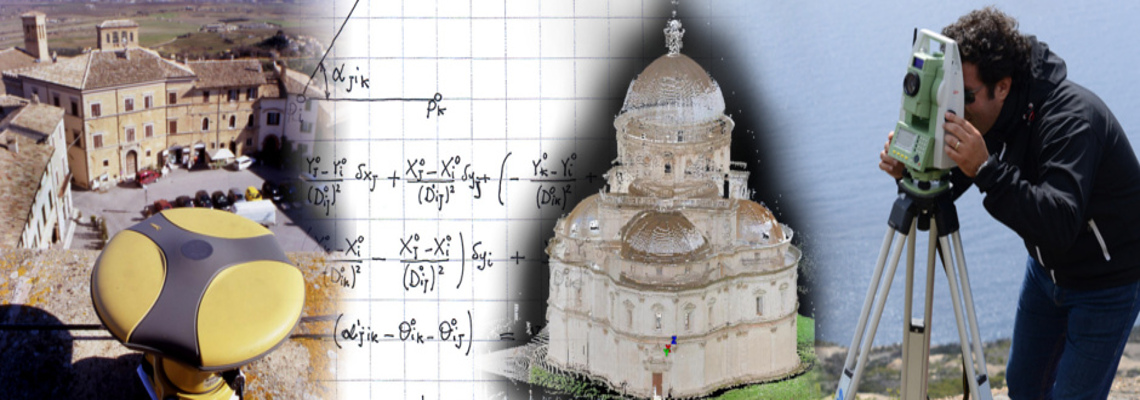
Radar Sensors
Sensors are are the first interface between the real word and the ICT world. among them motion sensors occupy a great role ranging form trafic control, presence detection and reaction (domotic, alarm set,...) to health (breath monitoring, localisation, assisted living, child monitoring,...). The experience gathered in the past, working in the automotive sector, is now exploited for intelligent lighting systems (see project ENLIGHT) by means of new technologies (SiPoP, inkjet printing,...) and materials (paper).
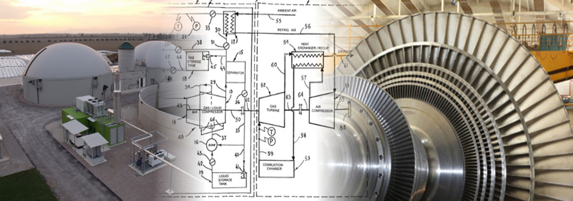
Microwave and millimeter-wave radiometers
Microwave and millimeter-wave radiometers are custom designed for several applications ranging from the early detection of fires to the measurement of Solar flares. Aside to the standard discrete-component approach, several System-on-Chip developments have also been conceived. Exploiting the latest generation of standard silicon processes, indeed, the integration of a complete millimeter-wave receiver is nowaday possible. Both SiGe and CMOS technologies are suitable for this purpose, this meaning that a full instrument (receiver, detector, calibration circuitry and ADC) can be miniaturized down to a single chip.
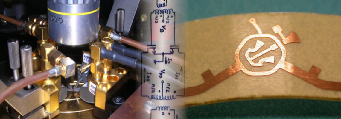
RFIC design
The RFIC design is carried-out exploiting silicon technologies. The following processes are available: SiGe 0.35um (from AMS foundry) and 0.25um (from IHP foundry); 90nm and 65nm CMOS (from both UMC and STM foundries). Multi-Project-Wafers (MPW) can be fabricated through various consortium such as Europractice and CMP. The design activity is mainly focused to the development of reconfigurable power amplifiers for WLAN applications and to the implementation of building-blocks for millimeter-wave radiometers.
Planar antennas
Planar antennas are designed and developed on "green substrate" such as the paper. These are suited for RFID applications as well as for short-range wireless sensors. Particular interest is devoted to "active antennas" i.e. antennas including oscillator or frequency multiplier circuits.